PCBs, or printed circuit boards, are a mainstay of modern technology. They are used in everything from cell phones to televisions to cars. But what exactly are PCBs, and how are they designed and assembled? This article will explore those questions in detail.
What are PCBs and what do they do?
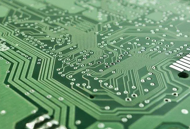
PCBs are electronic circuit boards. Comprised of many different electrical components, they serve as a medium for transmitting information or energy between multiple parts within an electronic device. They are unique in that they connect various types of modern technology, from cars to cell phones to computers. Assembly of a PCB is the first step in creating a functional part like a computer mouse. Getting PCBA Quotes from different companies will give you the best possible price. This way you can research different companies and the scope of their services for both prototype and production. A fast and detailed research option will sav you time (and money) so you can progress with your projects faster.
How are PCBs manufactured?
PCBs are assembled in several phases. After being designed via computer, they are made using a variety of techniques and with a variety of materials; most often with copper-clad boards and through chemical etching. When it comes to design, there is no single way to make a PCB, as there are many different techniques and materials available. Though there is no single standard for designing a PCB, there are certain design rules that should be followed to make sure the part can function properly and reliably. PCBs can be manufactured using several methods:
Chemical Etching
This method involves dissolving away copper to reveal conductive traces. This technique is the most popular, as it’s relatively quick and yields high-quality results.
Stamping
This process involves cutting out pre-made conductive paths from a roll of metal foil. It tends to be less expensive than chemical etching, but also of lower quality and is not very flexible.
Photolithography
This method involves exposing a light-activated resistance to UV light through a photomask. The pattern of the design on the mask is transferred onto the copper foil through an etching process that leaves exposed copper paths. While this method can produce high-quality, durable PCBs it is also very expensive.
Solvent Stamping
This method is similar to stamping, but it involves using a solvent to remove excess material from the copper foil before cutting it out. The excess material is removed during the development process through heat and pressure, thus creating a lower-cost product with high-quality results.
As far as materials go, any conductive material can be used; the most common materials are copper and nickel. To create a functional PCB, there need to be certain features present on the board. These include power buses, copper rings around bolts used for bolts securing components in place, ground connections between different components, and insulating material to protect circuits from short-circuiting
What are PCBA and SMT?
PCBA stands for printed circuit board assembly, and it is the process of assembling a PCB with components like resistors, capacitors, and integrated circuits. It also includes soldering these components to the board and adding wire connections between them.
PCBAs require very precise processes. There are also several different methods for PCBA, including:
Wave Soldering
In this process, solder is dropped onto a moving conveyor belt in a pattern that matches the design of the PCB. The board moves under it and the solder settles on all of the components and wires spread out on the surface. Then it passes through a wave of heat that melts the solder and attaches all of the components to their wires.
Pick and place
In this method, a robotic arm picks parts from a reeled strip and places them on a PCB one at a time. This yields very high accuracy and precision but is suitable for only smaller boards as it requires a great deal of labor.
Hand soldering
This is the least expensive and most time-consuming method, but it also yields high-quality results and allows for a large number of boards to be produced in a single day. This process involves placing components on the board by hand and then soldering them by applying solder with a heated iron or free from a solder pot.
PCBAs are only the first step in making a great electronic device. SMT stands for Surface Mount Technology, and it is used to place tiny components on the PCB, such as diodes, resistors, and other integrated circuits. These components need to be placed by an expensive machine that can hold just a few components at a time. SMT is faster than manual placement but also very expensive.
PCBAs are not limited to just electronics devices, they can be found in all kinds of products including toys, appliances, cars, and even children’s clothes. However, PCBs are mostly used for high-tech applications, where small size or weight is critical. Some examples of high-tech applications include cell phones, video game controllers, and disk drives.
PCBAs are an integral part of almost any electronic device. Their use has become widespread because they provide many advantages over other methods of building circuits. They produce better results than stamping or wire wrapping techniques, can be made in a variety of ways and on a variety of substrates, and can be produced cost-effectively.
The future of PCBs is very bright; they are constantly being improved to provide more capacity, better results, and lower production costs. Researchers are currently working on new techniques that will allow for multiple layer boards with fine connections, which means that complex circuits can be built into smaller devices than ever before. The PCB is one of the most important parts of any electronic device due to its ability to connect all of a product’s components. It has a wide field of applications from communication gadgets like phones and laptops, security to medicine, etc. Without a PCB, an electronic device would be very limited in what it could do or how much information it could hold.

PCBs are an integral part of almost any electronic device. Their use has become widespread because they provide many advantages over other methods of building circuits. They produce better results than stamping or wire wrapping techniques, can be made in a variety of ways and on a variety of substrates, and can be produced cost-effectively. The future for PCBs is very bright; they are constantly being improved to provide more capacity, better results, and lower production costs. Researchers are currently working on new techniques that will allow for multiple layer boards with fine connections, which means that complex circuits can be built into smaller devices than ever before.
Hey Everyone! This is Mia Shannon from Taxes. I'm 28 years old a professional blogger and writer. I've been blogging and writing for 10 years. Here I talk about various topics such as Fashion, Beauty, Health & Fitness, Lifestyle, and Home Hacks, etc. Read my latest stories.